ABSTRACT
This work has been focused on a deep and systematic study of the point-contact PseudoMOSFET characterization technique.
Firstly, theoretical models for the Pseudo-MOSFET have been described and developed for ultrathin Si wafers, and for those with also ultrathin BOX. They have been validated with several simulations. Then, some Pseudo-MOSFET samples with different thickness and surface (passivated/non-passivated) have been analyzed and characterized.
Later, the combination of the Split-C(V) technique with the Pseudo-MOSFET configuration has allowed to obtain the carrier mobility in bare SOI wafers as a function of the inversion charge. Nevertheless, since the evaluation of this parameter depends strongly on the value of the effective area considered for calculations, this area has been examined as a function of the characteristics of the set up configuration.
Taking into account the variability of the area with experimental configuration parameters, a mathematical model has been proposed to calculate the effective surface in any characterization scenario. The model has been verified with the experimental results.
On the other hand, the carrier mobility have been also studied in Pseudo-MOSFET samples. In order to achieve the optimum enhancement for the mobility, the specific values for the backgate bias have been calculated using Poisson-Schrödinger numerical simulations combined with Split-C(V) experimental results.
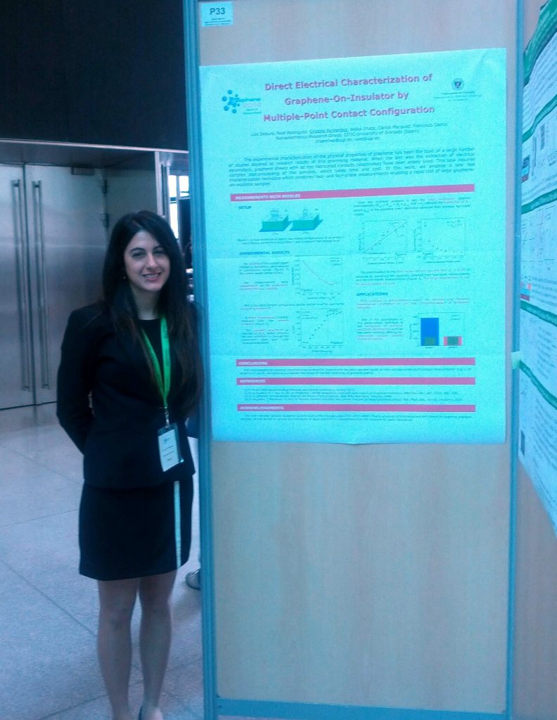
To conclude, new applications associated to point-contact techniques have been analyzed such us the use of the Pseudo-MOSFET as a sensor platform. In addition, several studies have been carried out on Poly-silicon or Graphene-On-Insulator samples demonstrating the flexibility of the point-contact methods to evolve with emerging substrates.


